- Posts: 40
Single-Board Universal Module
- moss
-
- Offline
A second filter can be thrown in if needed. The "filter" in the data sheet is just the typical buck output circuit. Leave room on PCB and populate if needed. There are also special SMT LC filters that may work. I kept it simple.
Please Log in or Create an account to join the conversation.
- PhracturedBlue
-
Topic Author
- Offline
- Posts: 4403
Please Log in or Create an account to join the conversation.
- octagon
-
- Offline
- Posts: 58
I guess you have the diode leakages under control.
Should additional filtering be needed, it looks like you could fit it on the layer one? A zero ohm jumper after the switcher can also be useful in troubleshooting, and can be used also for an inductor or a ferrite bead.
Nice work.
Please Log in or Create an account to join the conversation.
- mwm
-
- Offline
I'm not sure how legal this is, or if it would apply to the universal module, but if someone were serious about making and selling universal modules, it would probably be worth their while to discuss this option with a lawyer.
Do not ask me questions via PM. Ask in the forums, where I'll answer if I can.
My remotely piloted vehicle ("drone") is a yacht.
Please Log in or Create an account to join the conversation.
- PhracturedBlue
-
Topic Author
- Offline
- Posts: 4403
Please Log in or Create an account to join the conversation.
- Fernandez
-
- Offline
- Posts: 983
www.pololu.com/picture/view/0J3333
Please Log in or Create an account to join the conversation.
- octagon
-
- Offline
- Posts: 58
But from what I can see there are a couple of things I'd do differently.
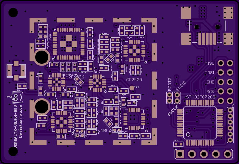
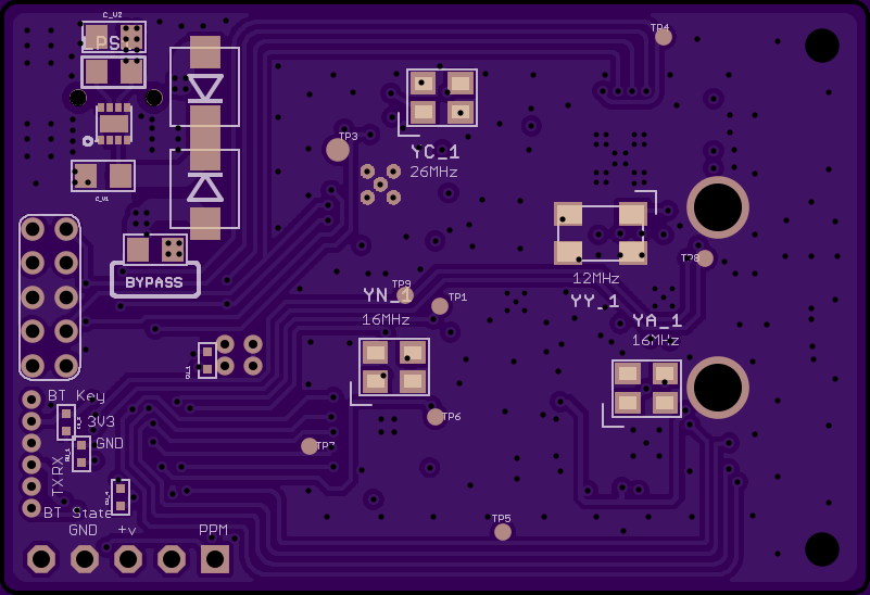
The footprint for the TPS62172 looks different than the datasheet, which also include two vias in the center pad. This I got burned on, trying to eliminate on this size part. With vias in the center pad excess solder will suck down the part to the pad, which otherwise may be rocking and rolling on the center blob, not making contact with an edge.
The two larger holes for the USB connector can be vias, tied to ground for better thermal and electrical grounding, I think these are holes for the plastic bosses in the USB connector.
The footprint geometry in the datasheet looks different, and I would follow it exactly, paste mask and all. There is not too much wiggle room on 2x2mm parts.
( Making the pads a little longer helps if you have to hit the lead-less part with a soldering iron tip.)
The traces on the VIN and EN can be combined and made wider, like the app-note.
The grounds on the CIN and COUT and very close to each other, there may be a circulating current between them so I'd keep the as close as possible.
Here is rough sketch.
Please Log in or Create an account to join the conversation.
- PhracturedBlue
-
Topic Author
- Offline
- Posts: 4403
I have tried doing a layout as you suggest, but I end up with a longer node attached to SW, and the loop from SW->L->Cvout->PGND is significantly longer. the layout guidelines do not specifically call out sharing the Vin and Vout cap gnd, but do indicate a single-point ground, as well as that the Vin Cap should be close to PGND and also (from above) that the Vout cap should be close to PGND.
getting vias on the pad will be challenging as well.
Here is what I was able to do (it isn't yet clean, just a proof of concept)
FYI, I used the SparkFun library for this device. I agree that it'd be better to use elongated pads like we did for the other QFN parts
Please Log in or Create an account to join the conversation.
- octagon
-
- Offline
- Posts: 58
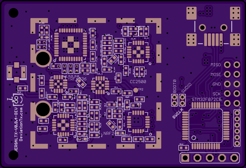
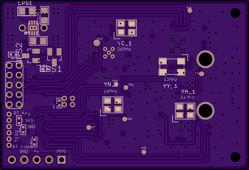
I did not update the PS1 lib's smd sizes, according to TI, just added two vias and a larger center pad.
USB holes I changed to (0.9mm) vias. Top side routing changed a little.
I'm ignorant of the mechanical constraints. Do you have a .step file of the case?
bitbucket.org/deviationtx
Please Log in or Create an account to join the conversation.
- PhracturedBlue
-
Topic Author
- Offline
- Posts: 4403
It looks good to me.
I don't have a case design. There aren't really any mechanical constraints other than thatthe board cannot shange size, and noen of the connectors can move. The USB can move a small amount if neededas it isn't critically placed, but I'd rather move it as littel as possible.
Please Log in or Create an account to join the conversation.
- octagon
-
- Offline
- Posts: 58
I could upload those files, but I want to fix that TI layout first.
Please Log in or Create an account to join the conversation.
- PhracturedBlue
-
Topic Author
- Offline
- Posts: 4403
Please Log in or Create an account to join the conversation.
- octagon
-
- Offline
- Posts: 58
If both supplies are ON, the the intrinsic diode takes over, cutting out like 0.55V. The file below can be used with LTspice.
Please Log in or Create an account to join the conversation.
- PhracturedBlue
-
Topic Author
- Offline
- Posts: 4403
Please Log in or Create an account to join the conversation.
- Jasenk
-
- Offline
- Posts: 84
- JustenCase
-
- Offline
- Posts: 13
Please Log in or Create an account to join the conversation.
- moss
-
- Offline
- Posts: 40
Of course with both power supplies active, the p-FET diode drop takes over.
Please Log in or Create an account to join the conversation.
- PhracturedBlue
-
Topic Author
- Offline
- Posts: 4403
Please Log in or Create an account to join the conversation.
- PhracturedBlue
-
Topic Author
- Offline
- Posts: 4403
Please Log in or Create an account to join the conversation.
- PhracturedBlue
-
Topic Author
- Offline
- Posts: 4403
The RFAxis comparative analysis recommends a TDK DEA162450BT-1260B3, however, Murata makes a LFB182G45SG9B740 with roughly similar specs which is much cheaper. I don't know how a band-pass filter will compare to the Pi-filter I've currently got on the output
Please Log in or Create an account to join the conversation.
-
Home

-
Forum

-
Development

-
Development

- Single-Board Universal Module


